The word sensor is used for an element produces a signal relating to the quantity which has to be measured. In most of the Cases, the transducer is used in place of the sensor. The use of sensors depending on the condition and system requirement.
In some system two and more than two sensors are used for;
Their signal conditioning in the combined package. Such type of system required further processing,
For that, it is suggested to have the sensor and
The signal conditioning grouped with a microprocessor
All in the same package to obtain the required result from all the constituents’ sensors at the same time. Such an arrangement is called a smart sensor.
To some extent, it is comparatively automated than the single sensor arrangement. Smart sensors can have such function as the ability to compensate for random errors,
To adopt changes in the surrounding and;
It gives the automatic calculation of the measurements’ accuracy,
Adjusts for non-linearity to produce a linear output, self-calibrated and give self-diagnosis of fault if any.
Before going in-depth about the sensor, let’s know the basic concept behind it. In the light sensor, semiconductor materials are used,
The electric conductivity of this material lies between the conductor and insulator.
Basically, these materials are used for the manufacturing of electronic components.
PN Junction diode
It is the combination of two semiconductor materials of an N-type
Semiconductor and P-type semiconductor. When these two materials are fused
It forms the semiconductor diode. The properties of the individual semiconductor get changed and
Produce very different properties than the parent materials. This diode is made up of the pieces of silicone having two terminals.
The first terminal is doped with P-type material and
The second terminal with N-type material. This PN Junction diode is a basic element for any semiconductor diode. This diode felicitated the migration of electron in one
Direction only and this is the main functions of the semiconductor diode. It is also used as a rectifier.
Types of light sensor:
- Photodiode
- Photo-transistor
- Photoresistor
1. Photodiode

It is a semiconductor device with PN junction and \,
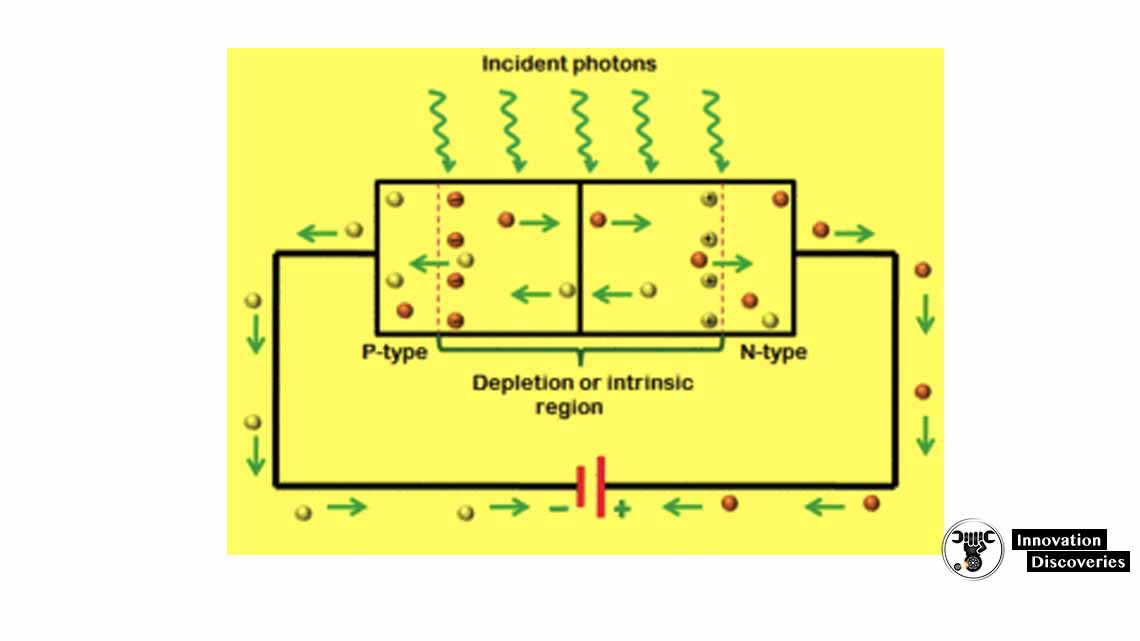
This PN junction layer found between the P-type semiconductor and N-type semiconductor. It is designed to work in the reverse bias mode. The photodiode has two terminals one is the anode and the second one is the cathode. In the forward bias condition, the current will flow from anode to cathode.
When the light falls the on the diode,
Couple of electron-hole formation takes place and,
This process is called the inner photoelectric effect.
Depletion region:
It is also called a depletion layer. As the word itself defines it that lack of something in the region. Depletion region where the doped semiconductor which is free to move to
Get diffused away or sometimes some external force is being applied to do so.
Ionized donor and acceptor impurities left in this region and there will be
No free electron to conduct the current as you can see in the above diagram. P3ositive charges are one side and negative charges are another side. This region forms the barrier and opposes the flow of current. To conduct the current external voltage is being supplied to break this barrier.
The light energy more than 1.1 eV strike on the diode to migrate the electrons from one region to another region. The intensity of the light energy absorption directly depends on the photons (unit of light). If the energy of the photon is lower, then the absorption will be deeper. When the photons strike on the PN Junction it gets illuminated. The light energy imparts their energy in the form of light to the PN junction. Because of this migration of the electrons take place from the valence band to
Conduction band and it leads to the flow of current. Hence photodiode converts light energy into electrical energy.
Applications
- Detection of both visible and invisible light rays.
- Used in digital and logic circuits.
- Used in optical fiber communication system.
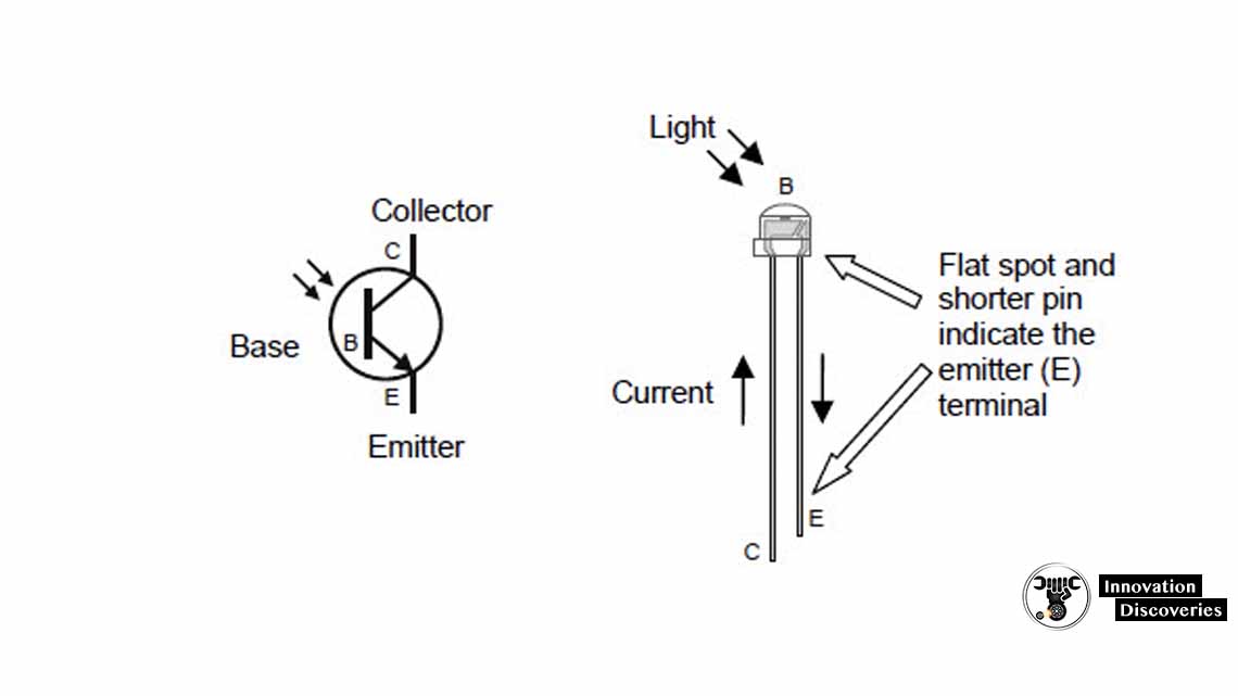
The phototransistor converts the striking light into photocurrent.
In this sensor, the light rays are used to illuminate the junction region
(Base region) instead of providing base current. It is consists of three-terminal, base, emitter, and collector. Base terminal is made up of the very special material
Which is sensitive to the light.
2. Phototransistor
The phototransistor converts the striking light into photocurrent.
In this sensor, the light rays are used to illuminate the junction region
(Base region) instead of providing base current. It consists of three-terminal, base, emitter, and collector. Base terminal is made up of the very special material,
Which is sensitive to the light.x

Silicon and other semiconductor materials are used for phototransistor and,
It is dependent on the light. It is generally encased in a transparent container to
Enhance light as it travels through it and allows you to reach the photosensitive region of the transistor. Its base is exposed to the light that amplifies the light which comes in contact with it. Because of this the relatively high current pass through the phototransistors,
As the current flow from base to the emitter,
Then the current is concentrated on it and converted into a voltage.
Applications
- Counting system
- Encoder sensing
- Object detection
- Ambient light detection
- Remote controller
- Read finger position
3. Photoresistor
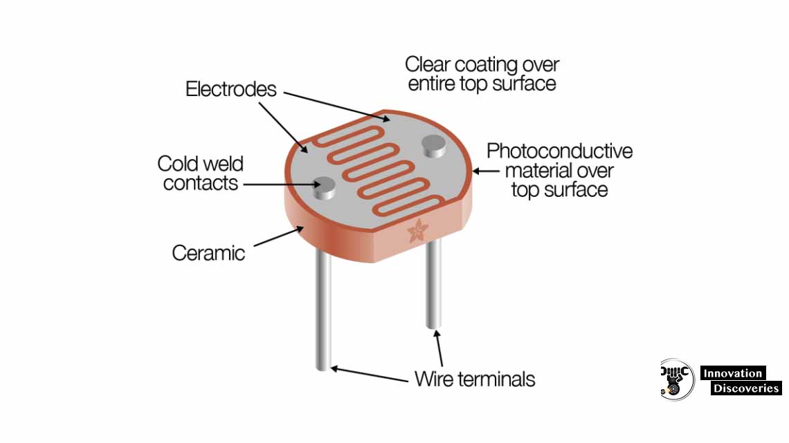
It is also known as the light-dependent resistor. It depends on the resistor, the flow of the current increases in photoresistor when the intensity of light increases.
As the name implies,
Photo means light and photon is the unit of light,
The resistor is the two terminals’ electrical component which implements current resistance as a circuit element. In this sensor, it used to reduce the current flow and adjust the signal level. It is a light-sensitive device used to indicate the presence and
Absence of the light and also used to measure the light intensity which falls on the surface.

Thes made up of lead sulphide, lead selenide,
Indium antimonide, cadmium sulfide, and cadmium selenide. It also made up of the semiconductor materials when the light strike on it some the valence electron
Which found free to move here and there absorbed some amount of heat energy,
And it leads to breaking the binding between the atoms.
The intensity of light and the free electrons are directly proportional to each other,
As the intensity of light increases, free electrons increases. Henc,e photoconductivity increases and it leads to a decrease in photo resistivity of the materials.
Applications
- Used to on and off the street light and it reduces the wastage of the electricity.
- Compare the relative light level.
- Light meters in camera.
- Used to control the reduction in the gain of the dynamic compressor.
- Infrared detectors.
It has lower sensitivity than the photodiode and the phototransistors. The photoresistor is dependent on the light. Two types of photoresistors are there in the market based on the material used in manufacturing are ‘intrinsic and extrinsic’. It is less costly than the photodiode and also it is less accurate.


One Comment